The 4067 was one of the IC’s that I wanted to connect up to various microcontrollers as it looke dextremely useful, here is a quick description from one of the datasheets with an overview of the functionality
The HEF4067B is a 16-channel analog multiplexer/demultiplexer with four address inputs (A0 to A3), an active LOW enable input (E), sixteen independent inputs/outputs (Y0 to Y15) and a common input/output (Z). The device contains sixteen bidirectional analog switches, each with one side connected to an independent input/output (Y0 to Y15) and the other side connected to the common input/output (Z). With E LOW, one of the sixteen switches is selected (low-impedance ON-state) by A0 to A3. All unselected switches are in the high-impedance OFF-state. With E HIGH all switches are in the high-impedance OFF-state, independent of A0 to A3. The analog inputs/outputs (Y0 to Y15 and Z) can swing between VDD as a positive limit and VSS as a negative limit. VDD to VSS may not exceed 15 V.
Here is a pinout of the IC
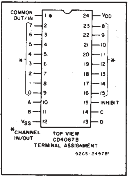
4067 pinout
And here is a truth table, by looking at this you can see that depending on the state of S0 – S3 and whether the enable pin is low will select one of the the channels. Now depending on pin 1 the current either flows in to be sent to one of the sixteen outputs – or the current flows out from one of the sixteen inputs. It depends whether its tied to 0v or 5v. If you used 5v on pin 1 then you could drive LEDs via the channel pins.
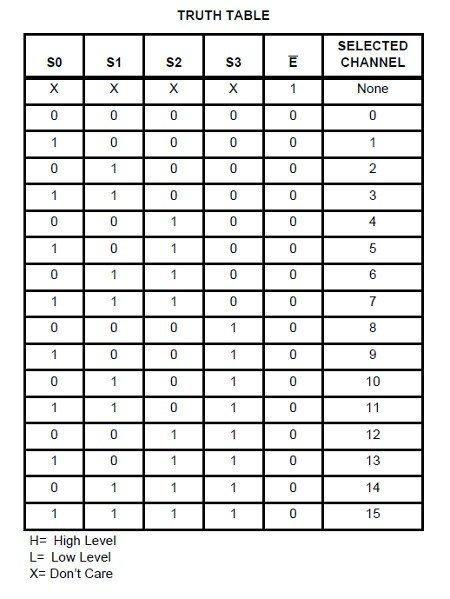
4067 truthtable
Schematic
Here is a schematic for a basic breakout, simply outputs the IC to various connectors
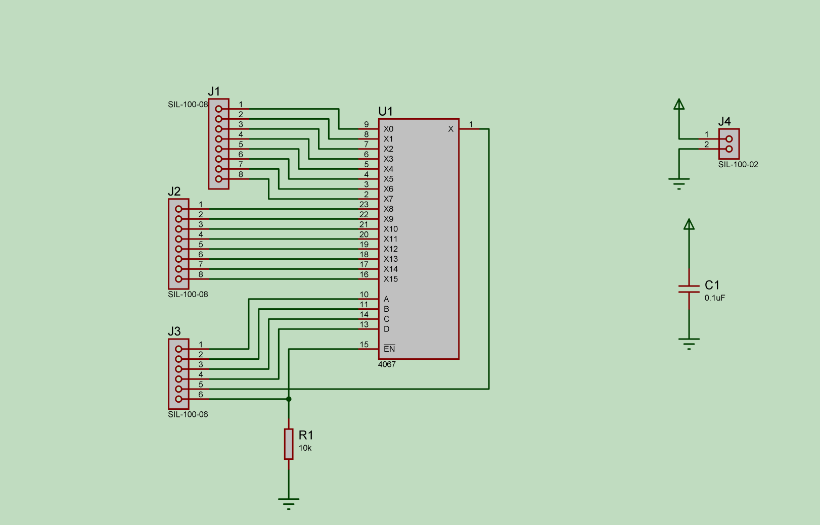
4067 breakout schematic
Layout
This was a sample layout I designed
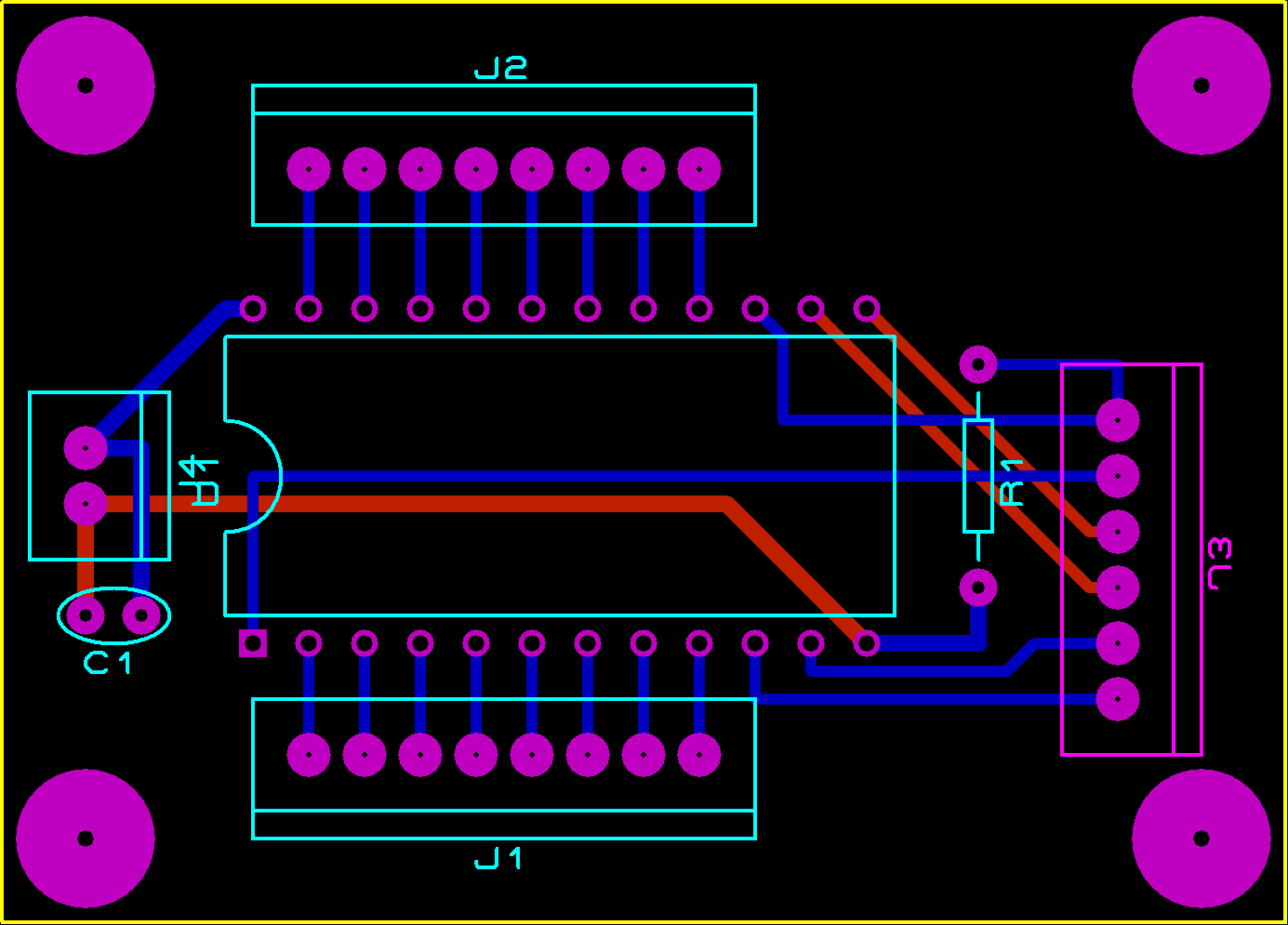
4067 breakout
Links
www.nxp.com/documents/data_sheet/74HC_HCT4067.pdf